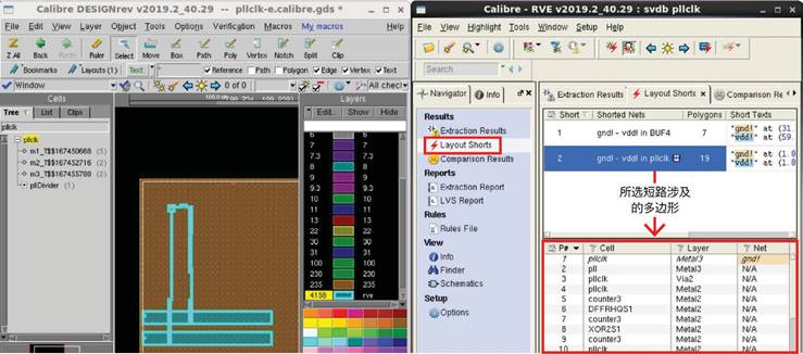
日本a√视频在线,久久青青亚洲国产,亚洲一区欧美二区,免费g片在线观看网站

        <style id="k3y6c"><u id="k3y6c"></u></style>
        <s id="k3y6c"></s>
        <mark id="k3y6c"></mark>


          <mark id="k3y6c"></mark>

          新聞中心

          EEPW首頁 > EDA/PCB > 設(shè)計應(yīng)用 > Dracula LVS介紹

          Dracula LVS介紹

          作者: 時間:2012-03-30 來源:網(wǎng)絡(luò) 收藏

          *input-layer

          pldd = 1

          contac = 3

          mt1 = 4 text 4 texttype 0 attach mt1

          thinox = 5

          nwell = 6 text 7 attach rnwel

          res = 7

          poly = 8

          dummy = 16

          substrate = bulk 99

          connect-layer = psub anwel pdiff ndiff poly mt1

          *end

          *oper

          not bulk nwell psub

          and poly thinox gate

          and gate dummy cgate

          not gate cgate agate

          and agate pldd pgate

          not agate pldd ngate

          not thinox gate diff

          and diff pldd pdiff

          not diff pdiff ndiff

          ;and contac pdiff pcont

          ;and contac ndiff ncont

          sel nwell cut res rnwel

          not nwell rnwel anwel

          and rnwel res wres

          not rnwel wres wress

          and psub pdiff pcont

          and anwel ndiff ncont


          關(guān)鍵詞: Dracula LVS

          評論


          相關(guān)推薦

          技術(shù)專區(qū)

          關(guān)閉